Projects
- K OTKA – Investigation of luminescence and ionization energy deposition processes in microstructured semiconductors based on neutral and charged particle conversion phenomena
- K OTKA – Information Processing with Resistive Switching Memory Devices
- TKP-VAX – Environmental monitoring sensors for emergency and extreme conditions
- OPERA – European Network for Innovative and Advanced Epitaxy
- Atomic layer deposition and applications of functional sulfide nanolayers
- INTAKE: Integrated Nanocomposites for Thermal and Kinetic Energy Harvesting
- Development of Nanometer Scale Resistive Switching Memory Devices
- Investigation of atomic or molecular processes induced by ultrashort laser and/or electron pulses
- KoFAH: Advanced Functional Materials for Autonomous Sensor Network
- HunQuTech: National Quantum Technology Program
- Deposition of ZnO and Ga2O2 nanostructures with atomic layer deposition
- PiezoMat: Ultra-high Resolution Pressure Sensing Uses Matrices of Vertical Piezoelectric Nanowire to Reconstruct the Smallest Features of Human Fingerprints
K OTKA – Investigation of luminescence and ionization energy deposition processes in microstructured semiconductors based on neutral and charged particle conversion phenomena
Span
2022-2026
Funding
NKFI K_22 CALL
Role
Project leader
PI
Zolnai, Zsolt
Summary
Nowadays microelectronics revolution leads to intensive size reduction meanwhile allows of increased density for data storage and improved spatial resolution for imaging devices. Besides such well-known areas, more special research tasks, like the detection of different charged and neutral particles, are also developing due to size reduction and increased efficiency.
Our aim is to construct and investigate 3D semiconductor-based micron-scale structures as neutron detectors utilizing appropriate particle-conversion mechanisms. The typically low-energy cold neutrons are captured by the carefully designed boron carbide component of the sample and up-convert their low energy by a factor of billion through the generation of high-energy particles which intensively deposit their energy to the solid via photon emission or electric charge generation, phenomena which lead to the detection of neutrons. Thanks to flexibility and precision of semiconductor technology, we can control the composition and 3D geometry of the detection volume on the micron-scale, the quantitative description of the underlying processes becomes possible and detection efficiency can be improved in a controllable way. Applying semiconductor boron carbide the spatial resolution for neutron imaging can be significantly improved as compared to that of Li- and He-based detection. The small-size mobile detectors besides state-of-the-art scientific applications may be utilized for meteorology, monitoring gates, localization of hidden radioactive sources, monitoring rock and soil moisture, or to find buried water sources on Earth or other planets.

Quantitative measurement of the Si and C content in SiC using 4He+ Backscattering Spectrometry analysis at (a) 3.55 MeV and (b) 1.5 MeV 4He+ ion beam energy.
K OTKA – Information Processing with Resistive Switching Memory Devices
Span
2022-2026
Funding
NKFI K_22 CALL
Role
Research Partner
MFA Coordinator
Pósa, László
Summary
The incredible progress of information technologies (IT) and the rapid growth of computing capacity is an everyday experience of our life. So far, this development was fueled by the miniaturization trend of the semiconductor industry. The demand for the analysis of enormously large datasets have resulted in an incredible progress of software technologies as well, especially in the field machine learning. On the other hand, semiconductor technologies clearly reach their limitations, and our data-intensive world seeks novel information processing architectures, that can complement or in some applications replace semiconductor circuits. The novel brain inspired computing solutions offered by the so-called resistive switching memory devices closely match the requirements for artificial intelligence tasks, and therefore this field of research and development is in the focus of most IT companies. Resistive switching memories, however, are not only promising hardware building blocks of large-scale artificial neural networks, but thanks to their complex behavior, circuits from a few resistive switching elements may already be able to recognize dedicated patterns in the input signal.
Throughout the project we will develop such novel sensing schemes, and we will build smart sensing circuits with the combination of artificial perception sensors and resistive switching architectures. Such signal detection schemes are especially useful in applications, where energy hungry and computation intensive digital circuits are better avoided, like artificial sensing interfaced to biological systems, or event-activated sensing tasks with poor energy resource.

Investigated Nb2O5-Ta2O5 filamentary (left), graphene-SiO2 phase change (middle), and VO2 phase change (right) type memristors
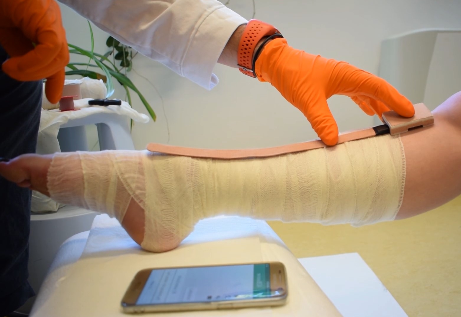
TKP-VAX – Environmental monitoring sensors for emergency and extreme conditions
Span
2021-2025
Funding
TKP2021-NVA-03
Role
PI
Principle Investigator
Volk, János
Summary
The development of sensors is typically a part of advanced electronics, in which today’s industrial and R&D capabilities enable Hungary to produce high value-added devices and their essential elements in the front end area.
The project aims at developing three families of sensors for monitoring the environment: i) vibration monitoring systems, ii) mobile gas detection, iii) gamma and neutron background radiation detectors. Using the unique infrastructure of the research centre in Hungary, sensor devices will be produced by researching new types of functional materials, developing and localising new micro- and nanotechnological processes, and demonstrating their operation by embedding them in electronics of our own design. Our R&D work is supported by our internationally recognised Materials Testing and Analysis Group.

Piezo-MEMS cantilevers for low acceleration vibration analysis
OPERA – European Network for Innovative and Advanced Epitaxy
Span
2021-2025
Funding
COST ACTION CA20116
Role
National Coordinator
Coordinator
Volk, János
Summary
The COST Action “European Network for Innovative and Advanced Epitaxy”, named OPERA, will build a new and innovative European Network composed of expert communities in epitaxial growth focusing on different materials classes: conventional semiconductors, oxides and 2D materials.
It aims to bridge the gap between traditionally separated scientific communities, both academic and industrial, having the common goal to combine complementary knowledge, push further the material maturation, and exploit epitaxial combinations of the different material classes in order to unveil new properties and produce new functionalities.
Based on this organization, the OPERA COST Action will foster interdisciplinary collaborative research activities allowing maintaining European epitaxy at the topmost worldwide level of research and innovation.

ZnO nanorod arrays grown by selected area wet chemical growth
Atomic layer deposition and applications of functional sulfide nanolayers
Span
2021-2025
Funding
National Research, Development and Innovation Fund (OTKA FK 139075)
Role
Leader
Project Leader
Baji, Zsófia
Summary
The aim of the present project is the atomic layer deposition of sulphides, and their applications in sensorics, optoelectronics, energy harvesting and storage. The ALD method of the targeted materials, FeSx, MoS2, TiS2, HfS2 and GaSx have only recently been developed, therefore the preparation itself, the optimisation of the deposition parameters is still a challenge. On the other hand all of these materials are important for a number of applications in energy storage and conversion and sensorics. The advantages of ALD, including the precise thickness and compositional control and the conformal coating of complex geometries, make it attractive for the surface engineering of devices.
Iron sulphide can be prepared in the form of FeS and FeS2. The latter is an especially important material for solar cell applications, as its absorbance is very high even in nanometre thickness. It is also a cheap and abundant material. Both FeS and FeS2 can be applied in water splitting both for hydrogen and oxygen generation.
MoS2 is a very versatile semiconducting material used in Li ion batteries as an electrode material, on the other hand, it can also be applied in water splitting for hydrogen generation. Its structure belongs to the transition metal dichalcogenide group. Titanium sulphide and hafnium-sulphide are also transition metal dichalcogenides with layered structures similar to that of MoS2 also very promising for a number of applications.
GaSx is a wide bandgap semiconductor with important photovoltaic and optoelectronic applications also depending on its stoichiometry and structure, and in its nanostructured form it is promising for water splitting as well.
HfS2 thin film deposited with ALD on a sapphire substrate
INTAKE: Integrated Nanocomposites for Thermal and Kinetic Energy Harvesting
Span
2021-2025
Funding
EU Research and Innovation Staff Exchange – RISE
Summary
INTAKE’s innovation vision aims to achieve a step change towards the
next generation of hybrid energy harvesting nanocomposites, which can be
integrated into lightweight and ultra-strong structural composites at
the nanoscopic level. This would infuse composite laminates with
inherent intelligent functionalities (such as energy harvesting, sensing
and wireless communication), without noticeable alterations or adverse
effects to the macroscopic structural properties.
Development of Nanometer Scale Resistive Switching Memory Devices
Span
2018-2022
Funding
National Research, Development and Innovation Fund (OTKA K 128534)
Summary
In this project we wish to develop, characterize and optimize novel ReRAM units. As a common approach of our studies we first engineer an initial on-chip structure fabricated by electron beam lithography, which is then further reduced in dimension by a controlled electrical breakdown process of the metallic terminals. The resistive switching is confined to the tiny volume of the substrate material residing under the resulting 1-3nm wide nanogap of the leads. This approach allows the study of ultrasmall ReRAM units well below the resolution of present lithographic techniques, which can also be integrated to larger circuits. In our studies graphene is considered as a distinguished material, providing a well shapeable, atomically thin, optically transparent and mechanically flexible contacting platform.
Investigation of atomic or molecular processes induced by ultrashort laser and/or electron pulses
Span
2018-2022
Funding
National Research, Development and Innovation Office, 2018-1.2.1-NKP-2018-00010
Role
Research Partner
Local Coordinator
Battistig, Gábor
Summary
The collaboration of the three institutions of complementary competencies develops a new tool able to study atomic and molecular processes triggered by the combined action of photons and electrons. The ultra-short pulses of electron needed for the processes will be produced by terahertz radiation. The new scientific tool is planned to setup and operate at ELI-ALP.
The task of MFA in the projectis is the fabrication of micro- and nano-sized structures and devices in which the electromagnetic field of terahertz radiation can accelerate electron packets with great efficiency. For the production and processing of semiconductor and dielectric structures in the required micrometer size range, only the MFA Microtechnology Laboratories provide the appropriate technology and expertise.
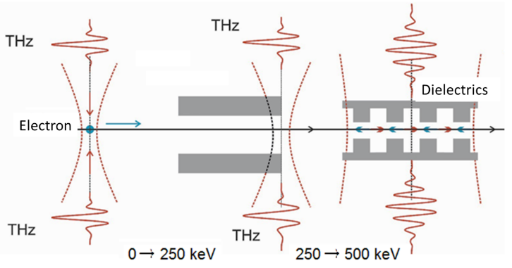
Principle of electron acceleration by electromagnetic field of THz radiation.
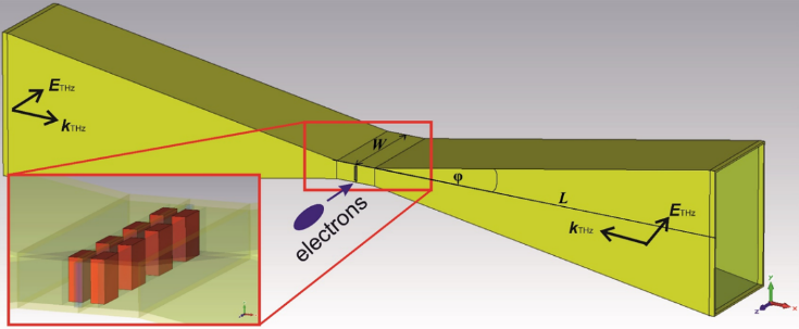
The planned setup: THz illumination of the dielectric microstructure (inset) trough the waveguides. The electromagnetic field on the structure accelerates the electron packets flying through the microstructure.
KoFAH: Advanced Functional Materials for Autonomous Sensor Networks
Span
2017-2020
Role
Leader
Project Leader
Volk, János
Funding
National Research, Development and Innovation Fund of the Hungarian Government (KoFAH, NVKP_16-1-2016-0018)
Summary
The aim of the KoFAH research project is to solve energy issues of Wireless Sensor Networks using advanced energy harvesting materials, low-power MEMS/NEMS devices, smart energy management, and highly efficient communication protocols. In the framework of the KoFAH program we target to upgrade our available systems and initiate the development of novel autonomous sensors.


HunQuTech: National Quantum Technology Program
Span
2017-2021
Funding
National Research, Development and Innovation Fund
Role
Research Partner (Nano circuit fabrication)
Local Coordinator
Volk, János
Summary
The National Research, Development and Innovation Office (NKFIH) facilitates the social and economic utilisation of discovery research findings by defining strategic areas where Hungary has the sufficient level of scientific excellence for the implementation of tasks, so that such goals can be reached faster and more efficiently. With this aim, the Office has announced the “National Quantum Technology Programme”, a funding source for consortia of research and knowledge-dissemination organisations and businesses involving research activities addressing large-scale interdisciplinary scientific and technological challenges which, due to their comprehensive nature and volume, are implemented in long-term cooperation between scientific, industrial and social stakeholders and decision-makers.
Deposition of ZnO and Ga2O3 nanostructures with atomic layer deposition
Span
2015-2020
Funding
National Research, Development and Innovation Fund (OTKA PD 116579)
Role
Leader
Project Leader
Baji, Zsófia
Summary
The project focuses on the deposition of ZnO and Ga2O3 thin films by ALD, their characterisation, and use in nanostructure fabrication.
ZnO is a wide band-gap semiconductor attracting considerable interest in the past few years due to its versatility in sensorics, optoelectronics, for transparent electrodes and thin film transistors. ZnO is commonly deposited by ALD, the process is well-established and -utilised in a number of applications. ZnO can easily be doped and alloyed by ALD as well, the most commonly used dopant being aluminum, although it has proven to be a less than perfect dopant. On the other hand the Ga doping of ZnO is a lot more promising, as it induces very high carrier concentrations, while leaving the crystallinity unaffected.
Gallium-oxide itself can not only be used as a dopant for ZnO, but is also a highly promising material in photocatalysis and sensorics. The atomic layer deposition method for Ga2O3 fabrication is fairly novel, therefore there are still a number of open questions about the technique itself, such as the use of the appropriate precursor, the deposition parameters, and the properties of the resulting layers.
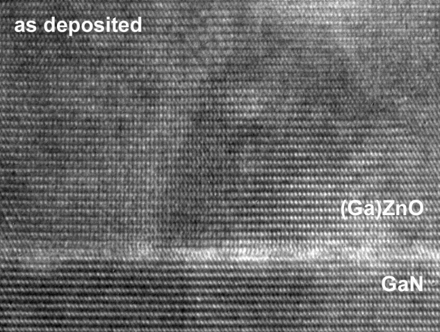
Ga doped ZnO deposited with ALD
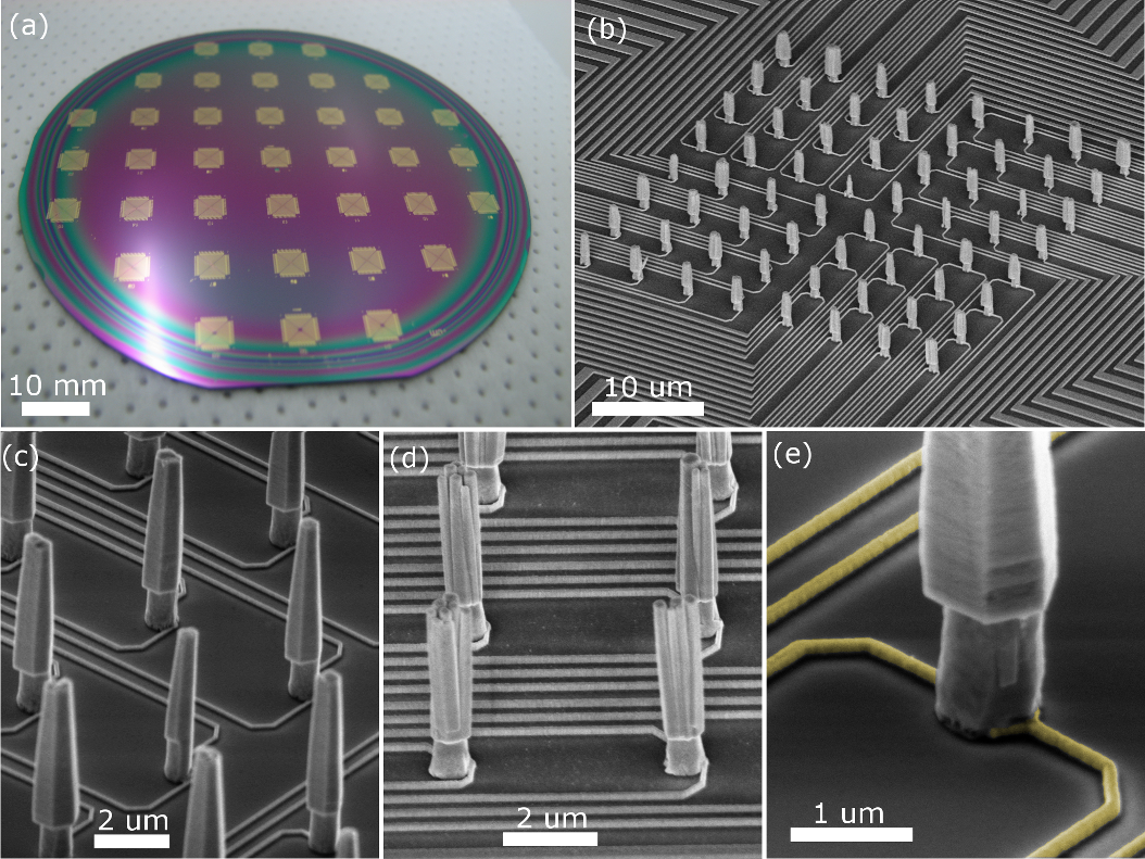
PiezoMat: Ultra-high Resolution Pressure Sensing Uses Matrices of Vertical Piezoelectric Nanowire to Reconstruct the Smallest Features of Human Fingerprints
Span
2013-2017
Funding
European Commission in the Seventh Framework Program (FP7, No 611019)
Role
Research Partner
Local Coordinator
Volk, János
Summary
PiezoMAT proposes a new technology of high-resolution fingerprint sensors based on a matrix of interconnected piezoelectric nanowires (NWs). The long term objective of PiezoMAT is to offer high performance fingerprint sensors with minimal volume occupation for integration into built-in systems able to compete on the market with the best existing products. PiezoMAT proceeds by local deformation of an array of individually contacted piezoelectric NWs and reconstruction from generated potentials, whose amplitudes are proportional to the NW displacement.